
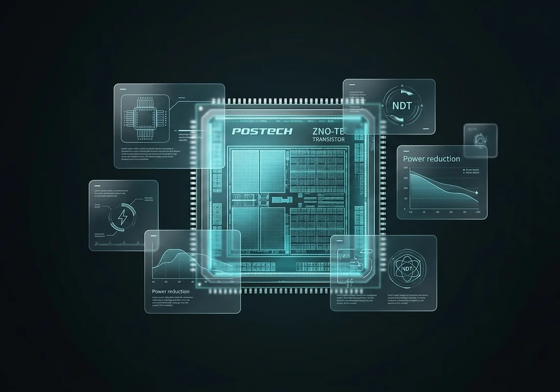
Innovations in Transistor Architecture from POSTECH
A group of researchers from South Korea’s POSTECH (Pohang University of Science and Technology) has introduced an innovative development that could radically change the approach to microchip design. They have developed a new type of transistor that significantly simplifies logic circuits, reducing the number of required components by up to 75%. This achievement was made possible by leveraging the unique properties of the heterojunction between zinc oxide (ZnO) and tellurium (Te), which exhibits the effect of Double Negative Differential Transmittance (D-NDT). This technology paves the way for creating more compact, energy-efficient, and performant chips, especially in the context of the growing needs of artificial intelligence and high-performance computing.
The modern semiconductor industry faces serious challenges related to the physical limitations of further transistor scaling. The traditional approach, based on Moore’s Law, requires placing an increasing number of transistors on a unit area, leading to a significant increase in power consumption and heat generation. The POSTECH development offers an alternative path: instead of simply reducing the size of individual elements, it allows performing complex logic operations using significantly fewer devices.
The Core of D-NDT Technology and the ZnO-Te Heterojunction
The key element of the new development is the use of a specific material – the heterojunction of zinc oxide and tellurium. This material exhibits the negative differential transmittance (NDT) effect, which means that within a certain voltage range, the current through the device begins to decrease as the voltage increases. The uniqueness of the POSTECH transistor lies in the fact that it exhibits double negative differential transmittance (D-NDT), allowing a single device to implement multi-valued logic equivalent to the operation of several traditional transistors.
The research team led by Professor Jang-Kyung Kim and Professor Seung-Ki Joo from the Department of Materials Science and Engineering at POSTECH was able to precisely tune the energy bands at the ZnO and Te interface. This allowed obtaining a stable and reproducible D-NDT effect at room temperature. The ZnO-Te heterostructure ensures unique carrier transport where electrons and holes tunnel through the barrier, creating a non-linear current-voltage characteristic.
Efficiency and Benefits: 75% Reduction in Components
Traditional logic gates, such as NAND or NOR, which form the basis of all digital computing, require the use of multiple transistors (typically from two to six for basic operations). A D-NDT based transistor can perform these operations using only one device. Consequently, when designing complex microchips, the overall number of components can be reduced by 75%.
This reduction offers a number of important advantages:
- Reduced chip area: Fewer components allow placing more functional blocks on the same area or making the chip significantly more compact.
- Energy efficiency: Fewer transistors mean lower power losses for switching, which is particularly important for mobile devices and data centers.
- Lower manufacturing cost: Simplifying the architecture and reducing chip area potentially lowers the production cost of each unit.
- Increased performance: Shorter signal paths and fewer switchings can lead to an increase in data processing speed, estimated by researchers to be four times faster.
It is worth noting that the POSTECH transistor demonstrates high stability and can operate at temperatures up to 100°C, making it suitable for use in real-world electronics operating conditions. The technology is also compatible with existing semiconductor manufacturing processes, facilitating its potential implementation.
Potential for AI and Future Computing
The new development holds particular promise for creating artificial intelligence (AI) chips. Modern AI algorithms require performing a massive number of computations, leading to high power consumption of AI accelerators. The architecture simplification and increased energy efficiency offered by the POSTECH transistor could significantly improve the performance of AI systems.
The POSTECH research is an important step in the development of semiconductor technologies. It demonstrates that innovations in materials science and device design can offer solutions to overcome the limitations of traditional scaling. While the technology is still in the laboratory research stage, its potential to reshape microchip architecture is significant. Further research will be aimed at scaling the technology, integrating it into complex logic circuits, and exploring mass production capabilities.




0 Comments