- Overcoming the physical limitations of silicon
- How the first 2D CMOS computer works
- Molybdenum disulfide and tungsten diselenide: a perfect pair
- Manufacturing technology and architecture
- Energy efficiency as a key advantage
- Prospects and future of microelectronics
- Applications of monatomic materials
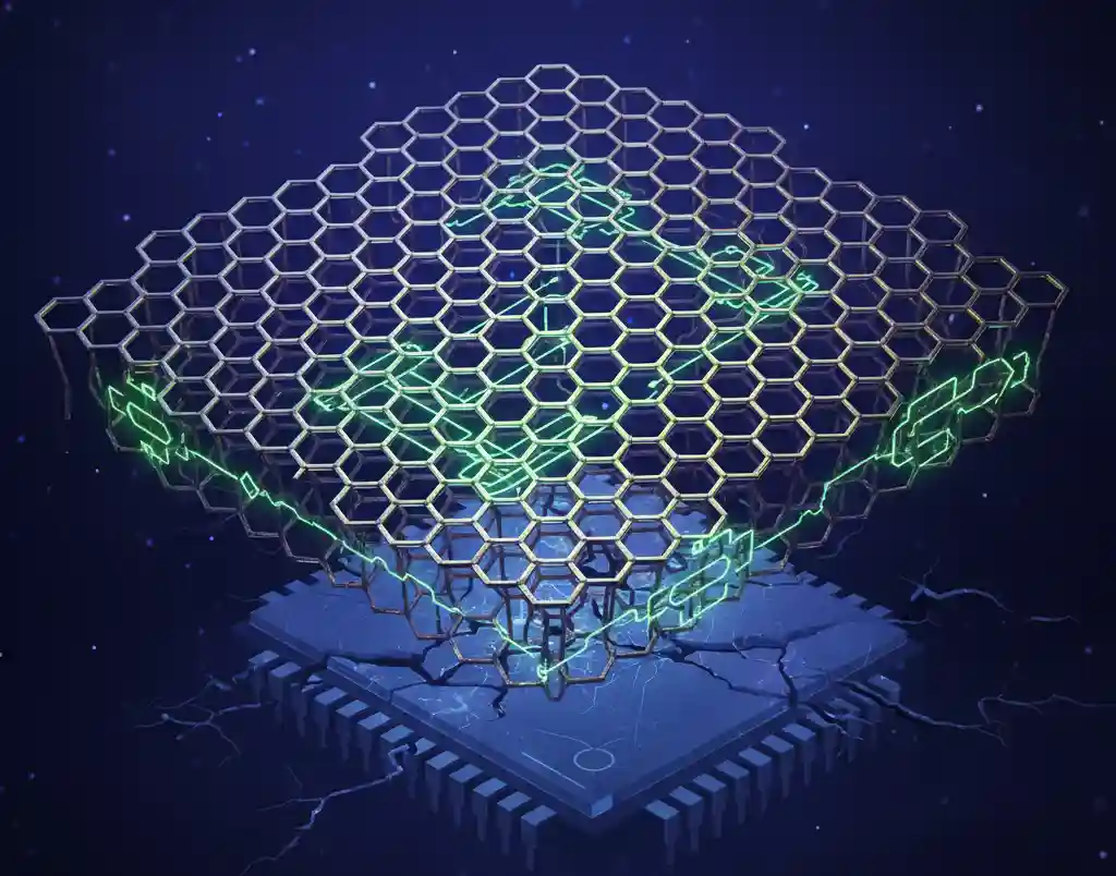
The scientific world is on the brink of revolutionary changes that could end the sixty-year dominance of silicon. Researchers from Pennsylvania State University (USA) have made a breakthrough, unveiling the world’s first functional silicon-free computer. This prototype is built entirely from 2D materials just one atom thick, opening up incredible prospects for the miniaturization of electronics.
Overcoming the physical limitations of silicon
The era of silicon, which spawned a revolution in information technology, is approaching its physical limits. Moore’s Law, which for decades dictated a doubling of the number of transistors on a chip, is now running up against the fundamental limitations of the material. As silicon components shrink to nanoscale (less than 5 nanometers), their performance deteriorates sharply. A so-called tunneling effect occurs, where electrons begin to “penetrate” through ultra-thin barriers, increasing energy consumption and heat generation. Therefore, the search for an effective alternative to silicon has become a priority for research centers worldwide.
How the first 2D CMOS computer works
A key achievement was the creation of a working complementary metal-oxide-semiconductor (CMOS) circuit without silicon. CMOS technology is the foundation of the vast majority of modern electronic devices, from smartphones to servers. A team led by Professor Saptarshi Das replaced a traditional semiconductor with two different single-atom materials, effectively combining them to form the necessary n-type and p-type transistors.
Molybdenum disulfide and tungsten diselenide: a perfect pair
- Molybdenum disulfide (MoS_2) has been used to create n-type transistors that produce negatively charged electrons.
- Tungsten diselenide (WSe_2) was used to create p-type transistors that produce positively charged “holes” (charge carriers).
These 2D materials have a unique property: unlike bulk silicon, they retain their exceptional electronic properties even in layers just one atom thick. This allows for the creation of extremely thin and energy-efficient logic elements.
Manufacturing technology and architecture
To fabricate computer components, the researchers used metal-organic chemical vapor deposition (MOCVD). This technology is critically important because it enables the growth of atomic-thin materials with high purity and control on a large scale.
- In total, more than 2000 transistors were produced, integrated into a single circuit.
- On their basis, a full-fledged, albeit basic, “single instruction set computer” (OIC) was created.
- The computer demonstrated the ability to perform simple logical operations such as addition, multiplication, as well as memory operations (writing and reading).
Although the first prototype’s performance is limited to 25 kilohertz, significantly slower than modern chips with gigahertz frequencies, this isn’t the key metric. The main breakthrough is the proof of concept: for the first time in history, a fully functional computer has been created without silicon, using only single-atom materials.
Energy efficiency as a key advantage
The main advantage of the new 2D CMOS chip is its incredible energy efficiency. Modern silicon devices, especially mobile ones, constantly require improved cooling systems and larger batteries due to increasing power consumption. The new silicon-free computer operates at a very low supply voltage, ensuring minimal power loss and heat generation.
- Reduced power consumption is critical for wearable electronics, medical implants, and autonomous sensors.
- Potentially, devices based on 2D transistors could require much smaller batteries or could function by harvesting energy from the environment (such as radio waves or light).
This innovation addresses an increasingly pressing issue: how to ensure continuous growth in computing power without dramatically increasing power and cooling requirements. Scientists are confident that further improvements in manufacturing technologies will bring the speed and performance of silicon-free transistors to competitive levels.
Prospects and future of microelectronics
The successful creation of the first 2D computer marks the beginning of a new era in semiconductor technology. This achievement doesn’t simply replace one material with another; it opens the door to fundamentally new forms of electronics.
Applications of monatomic materials
- Flexible Electronics: With atomic thickness, these 2D materials are ideal for creating flexible, transparent, and stretchable displays and devices that can be integrated into fabrics or worn on the skin.
- High-speed, low-power chips: Further research will optimize these silicon-free transistors for high-performance computing and low-power centers.
- Sensors and IoT (Internet of Things): The high sensitivity of single-atom materials allows for the creation of ultra-precise sensors for environmental monitoring and biomedical parameters.
While scientists are also exploring other silicon alternatives, such as boron arsenide and gallium oxide, the development of a working 2D CMOS computer has become the most compelling evidence yet that the future of microelectronics lies beyond traditional 3D materials. Given the significant investment and publication of the results in the influential journal Nature, we can expect rapid advances in this technology over the next decade.


0 Comments