
- A Shift in Flagship Silicon Architecture
- Architectural Overview and Hardware Specifications
- CPU Processing Performance and Thermal Behavior
- Xclipse 960 Graphics Architecture and Hardware Ray Tracing
- Constrained Power Profile Analysis
- Neural Processing Unit and Edge AI Acceleration
- Power Consumption and Thermal Envelope Management
- Market Implications for Mobile Platforms
A Shift in Flagship Silicon Architecture
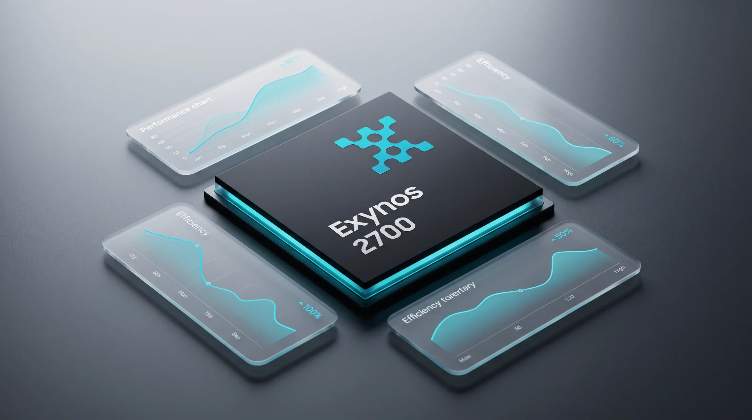
The mobile semiconductor sector has officially reached commercial implementation of sub-3nm nodes. For several product generations, Samsung System LSI trailed behind Qualcomm Snapdragon platforms in sustained power efficiency, thermal throttling mitigation, and peak GPU output. The latest internal validation telemetry for Exynos 2700 engineering samples indicates a measurable performance transition against the competing Snapdragon 8 Elite Gen 6 Pro platform.
This efficiency progression stems from the mature deployment of Samsung Foundry’s SF2P fabrication standard utilizing third-generation Gate-All-Around nanosheet field-effect transistors. By controlling sub-threshold leakage currents across dense logic gates, the platform achieves higher operational clock ceilings without surpassing standard thermal envelope thresholds in slim smartphone designs.
Architectural Overview and Hardware Specifications
While both silicon solutions utilize modern compute blocks, their topology demonstrates opposing design methodologies. Samsung employs a balanced ten-core tri-cluster CPU arrangement, whereas Qualcomm relies on a dual-cluster configuration powered entirely by proprietary third-generation Oryon performance cores.
The lower production bill-of-materials cost of 175 USD provides substantial integration flexibility for commercial device assembly. In contrast, Qualcomm unit pricing remains elevated past 230 USD, which creates margin constraints for device manufacturers evaluating multi-tier component supply chains.
CPU Processing Performance and Thermal Behavior
In standard Geekbench multi-threaded evaluation runs, pre-production Exynos 2700 hardware records an overall throughput advantage of 9.5%. This compute gain is facilitated by fine-grained thread allocation managed by an upgraded Energy Aware Scheduling implementation directly integrated into the platform kernel.
- Single-Threaded Workloads – Snapdragon maintains a slight 2.1% advantage due to elevated L2 cache sizing on its dedicated primary core.
- Multi-Threaded Workloads – Exynos establishes an advantage via ten concurrent hardware execution threads and minimal throttling variance.
- Memory Subsystem – The integrated LPDDR5X-9600 controller supports peak system memory bandwidth reaching 76.8 GB/s with reduced read-write latency.
Thermal stability profiles show substantial mitigation of frequency decay. While earlier iterations experienced frequency cuts reaching 25% under extended stress profiles, the SF2P node sustains operational limits with a minor 6% throttling drop across continuous 30-minute stress loops.
Xclipse 960 Graphics Architecture and Hardware Ray Tracing
The continuing engineering collaboration with AMD delivers tangible improvements for high-end mobile 3D rendering. The integrated Xclipse 960 GPU leverages custom RDNA 4.5 compute units, prioritizing hardware-accelerated BVH traversal and AI-assisted temporal upscaling routines.
Constrained Power Profile Analysis
Under a strict power clamp of 2.5 W within the 3DMark Wild Life Extreme stress loop, the Xclipse 960 graphics block delivers an average framerate of 48.2 FPS. The competing Adreno 840 Pro delivers 44.1 FPS under identical power constraints, illustrating architectural efficiency gains when operating within restricted thermal envelopes.
Hardware Machine Learning Super Resolution integration allows the pipeline to process assets internally at sub-native resolutions before presenting high-fidelity Quad HD+ frame outputs with minimal latency overhead.
Neural Processing Unit and Edge AI Acceleration
Modern mobile platforms require local compute acceleration for transformer architectures. The integrated NPU inside Exynos 2700 utilizes wide dual-precision tensor arrays capable of direct FP8 and INT4 mathematical operations.
- Local inference processing for 7B parameter foundation models reaches 24 tokens per second without network access.
- Complex multimodal processing tasks execute 18% faster compared to Qualcomm hardware alternatives.
- Idle power consumption for always-on contextual perception layers remains below 45 mW.
These dedicated processing pipelines ensure complex contextual services run on-device, preserving privacy requirements while eliminating background battery drain during idle states.
Power Consumption and Thermal Envelope Management
Power efficiency metrics remain the primary benchmark for consumer hardware deployment. Using hardware oscilloscope data acquisition systems, test hardware registered 161 mA for the Samsung platform versus 185 mA for the Qualcomm solution under standardized cyclic compute workloads.
This 12.7% power efficiency differential translates to measurable runtime expansion during prolonged high-load scenarios. Furthermore, total silicon die area was reduced by 8% relative to previous generation tape-outs, enabling efficient vapor chamber packaging within compact chassis designs.
Market Implications for Mobile Platforms
Competitive validation of internal silicon alters future component procurement dynamics for tier-one smartphone releases in 2027. Re-establishing parity enables manufacturers to balance supplier dependencies while insulating device pricing against shifting licensing structures.
For end consumers, these architectural results point toward reduced performance disparity between regional device variants. Should production yields mirror early validation telemetry, upcoming flagship hardware will deliver uniform gaming, processing, and battery longevity standards globally.




0 Comments